Let's explain to Junior high school students simply! What is a 2-nanometer semiconductor?
2025.03.03
- LSI Circuit Design
Have you heard the term "2-nanometer semiconductor" often featured in the news? Simply put, they are "electronic circuits made from ultra-narrow semiconductor elements measuring 2 nanometers." Although it's sounds like a difficult name, they are deeply involved in our daily lives. In this article, we'll explain "2-nanometer semiconductors" in easily.
What is a nanometer?
Nano is a prefix attached to units that represent a certain quantity. It means "one billionth" or "10 to the -9 power". Nanometer is a unit that represents one nano (one billionth of a meter) of the SI (International System of Units) base unit of "meter".
First, mm (millimeter) represents one thousandth of a m (meter). Milli means 10 to the -3 power.
Next, one thousandth of a mm (millimeter) is called a μm (micrometer). μ (micro) represents 10 to the -6 power.
And one thousandth of a μm (micrometer) is called a nm (nanometer).
* μm (micrometer) was formerly called μm (micron).
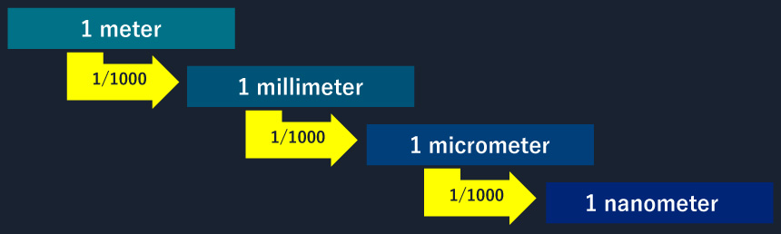
Figure 1. Scale of a nanometer
2nm (nanometer) represents an extremely short length that 2 billionths of a meter, or 2 millionths of a millimeter, or 2 thousanths of a μm (micrometers). The average hair of a Japanese woman is 0.08mm thick.
This is equivalent to 80μm or 80,000nm. In other words, 2nm is 1/40,000th the thickness of a human hair. If a human hair were 400m thick, 2nm would be 1cm.
The size of a virus is said to be about 1/10,000mm, so 2nm is even smaller than a virus, and its length is 1/50th the length of a virus. This should make it easier to imagine the ultra-narrowness of 2 nanometers. For your information, 2nm is equivalent to 20Å (angstroms). Angstroms are also used in textbooks as a unit of measurement for the size of atoms and molecules.
What is a semiconductor?
Here's a brief explanation of semiconductors. First, imagine a "Switch".
The Figure below is a "Switch" made from semiconductor elements. Figure 2: MOS Transistor (Switch Off): In this state, the Switch is off, and no current flows. Figure 3: MOS Transistor (Switch On): Here, the switch is on, current to draw from the positive (+) to the negative (-) terminal.
The Figure below is a "Switch" made from semiconductor elements. Figure 2: MOS Transistor (Switch Off): In this state, the Switch is off, and no current flows. Figure 3: MOS Transistor (Switch On): Here, the switch is on, current to draw from the positive (+) to the negative (-) terminal.
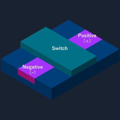
Figure 2: MOS Transistor (Switch Off)
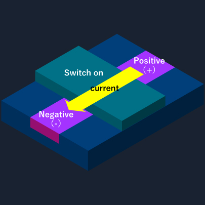
Figure 3: MOS Transistor (Switch On)
This "Switch" is called a "Transistor." Transistor is a coined word meaning "moving Resistor." This type of transistor is called a MOSFET.
Semiconductors and nanometers
The reason why "narrowness" is important in semiconductors is because transistors have a length (L) and a width (W), as shown in Figure 4.
These length (L) and width (W) represent the "Size" of a transistor. (They also represent performance, but we won't get into that here.)
These length (L) and width (W) represent the "Size" of a transistor. (They also represent performance, but we won't get into that here.)
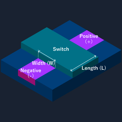
Figure 4. MOS transistor length (L) and width (W)
The length (L) and width (W) are expressed in "units" such as nm (nanometers) and μm (micrometers). The manufacturing process for semiconductors is called a "process," and one important aspect of this is the minimum length (L) of a transistor. This value is a standard that indicates how small a transistor can be made. Each process has a minimum value for the length (L) of a transistor, and there is a rule that "transistors with a length (L) shorter than this minimum value must not be made." For this reason, the length (L) of the transistor is used in the name of the process.
For example, a 45-nanometer process means that semiconductors are manufactured with a minimum transistor length (L) of 45 nm.
For example, a 45-nanometer process means that semiconductors are manufactured with a minimum transistor length (L) of 45 nm.
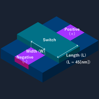
Figure 5. 45-nanometer process MOS transistor
An index that shows the miniaturization of semiconductors, including length (L), such as "nanoprocess," is called a "process node." The smaller the process node number, the more transistors can be placed on the chip, improving performance and efficiency. Will explain in "Semiconductors and Processes", process node name that use length (L) will no longer be used after a certain point.
Semiconductors and Electronic circuits
By combining transistors, we can create electronic circuits such as digital circuits and analog circuits. Here, we will briefly explain the logic elements used in digital circuits. By combining transistors as shown in Figures 6, 7, and 8, we can create the basis of the three basic logic elements of digital circuits: AND, OR, and NOT.
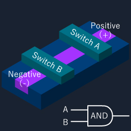
Figure 6. Logic element AND
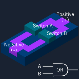
Figure 7. Logic element OR
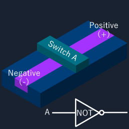
Figure 8. Logic element NOT
In principle, any digital circuit can be created by combining these three logic elements. For example, addition circuits, multiplication circuits, division circuits, and comparison circuits. The "CPU" inside your computer or smartphone is also made by combining these circuits. CPU stands for Central Processing Unit, which means "central processing unit."
Example of an adder circuit constructed using logic elements
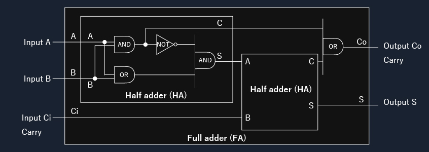
Figure 9. Half adder (HA) circuit and full adder (FA) circuit
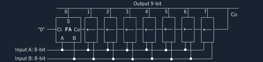
Figure 10. 8-bit addition circuit
Here is a simple explanation of how Figures 9 and 10 to work.
| Input signal | 8-bit digital signals A and B to be added are input. |
|---|---|
| Half adder (HA) |
|
| Full adder (FA) |
|
| 8-bit addition circuit | This circuit connects 8 full adders (FA) by carry (Figure 10). Adds 8-bit input A and 8-bit input B and outputs a 9-bit value including the 1-bit carry. |
The real circuit is very complicated, but we have explained the principle here. Semiconductors are found in the electronic devices that we use, such as the televisions and air conditioners, as LSIs (large-scale integrated circuits).
These LSIs contain silicon chips that are just a few millimeters square, small enough to fit on the tip of a finger. The surface of these silicon chips is densely packed with electronic circuits made up of transistors.
These LSIs contain silicon chips that are just a few millimeters square, small enough to fit on the tip of a finger. The surface of these silicon chips is densely packed with electronic circuits made up of transistors.
Semiconductors and Processes
The history of semiconductors has seen the evolution of process technology. Process technology is the pursuit of "how small and high performance semiconductors can be made." Semiconductors, which first appeared in the 1960s, have become smaller and more powerful over their long history.
Here, we will look at their evolution using Intel's CPU as an example.
Here, we will look at their evolution using Intel's CPU as an example.
| Year | Process node | CPU name | Transistor count |
|---|---|---|---|
| Micron era | |||
| 1971 | 10μm | 4004 | 2,300 Transistor |
| 1974 | 6μm | 8080 | 6,000 Transistor |
| 1976 | 3μm | 8085 | 6,500 Transistor |
| 1978 | 3μm | 8086 | 29,000 Transistor |
| 1982 | 1.5μm | 80286 | 134,000 Transistor |
| 1985 | ~1μm | Intel386 | 275,000 Transistor |
| The Submicron Era | |||
| 1989 | ~0.6μm | Intel486 | 1,200,000 Transistor |
| 1993 | ~0.35μm | Pentium | 3,100,000 Transistor |
| The deep submicron era | |||
| 1997 | ~0.18μm | Pentium Ⅱ | 7,500,000 Transistor |
| 1998 | ~45nm | Celeron | |
| 1999 | ~0.13μm | Pentium Ⅲ | 9.500,000 Transistor(except 512KB L2_Cache 25,000,000 Transistor) |
| 2001 | ~90nm | Itanium | |
| 2006 | ~45nm | Intel Core2 Duo | |
| FinFET Era | |||
| 2012 | 22nm | 3rd Generation Intel Core (3D Tri-Gate Transistor/FinFET) | |
| 2014 | 14nm | Intel Core M | |
| 2019 | 10nm | 10th Generation Intel Core | |
Intel Corporation. "Intel's History".https://www.intel.co.jp/content/dam/www/central-libraries/jp/ja/documents/2022-05/history-of-intel-jp.pdf,(referred 2024-07-19)
Wikipedia.「Pentium III」.https://en.wikipedia.org/wiki/Pentium_III,(referred 2024-07-19)
* "~" indicates that the device is also being produced more large process node.
Wikipedia.「Pentium III」.https://en.wikipedia.org/wiki/Pentium_III,(referred 2024-07-19)
* "~" indicates that the device is also being produced more large process node.
Transistor structure is beginning to transition from the conventional MOSFET shown in Figure 11 to the FinFET shown in Figure 12.
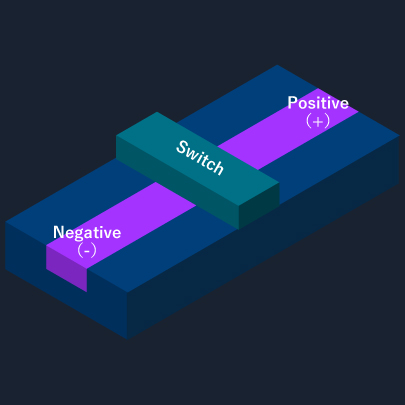
Figure 11. Planar type MOSFET
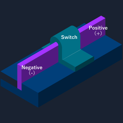
Figure 12. FinFET
In the future, semiconductor manufacturers aim to evolve their processes to 10nm, 7nm, 3nm, 2nm (20Å), and 1nm (10Å). Up until the 3nm process, FinFETs have been widely adopted as the mainstream transistor structure at many foundries. From the 2nm process onwards, it is expected that there will be a transition to the GAA (Gate-All-Around) structure shown in Figure 13.
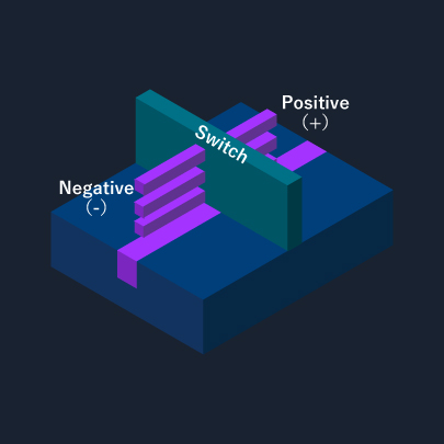
Figure 13. GAA
Transistor structure will also undergo various changes.
By 2024, miniaturization will have progressed to around 3nm. The name of the process node "3nm" no longer directly represents the physical length (L) of a transistor, since transistors with a three-dimensional structure called FinFET became mainstream. Currently it seems to indicate that a level of performance and miniaturization equivalent to the 3nm process has been achieved.
It's likely that in the future we will move away from using "length" in process node names. Intel have used process node names such as Intel7 and Intel3.
The amazing 2-nanometer semiconductors
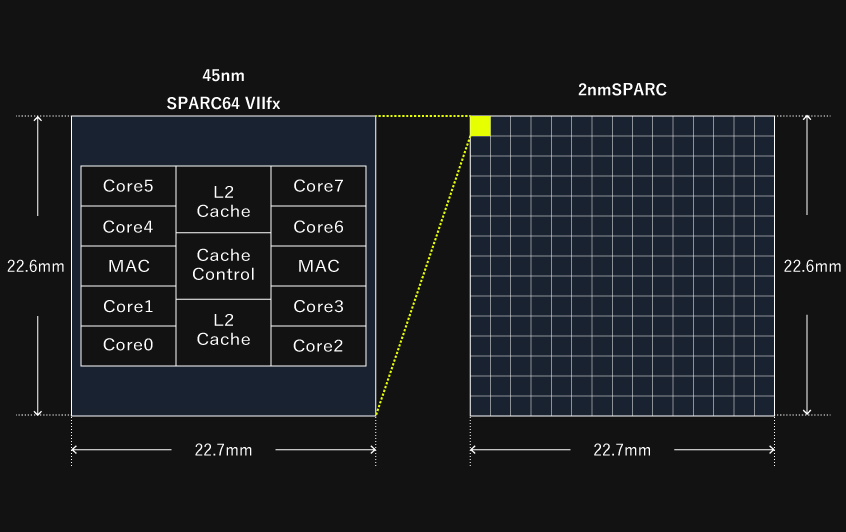
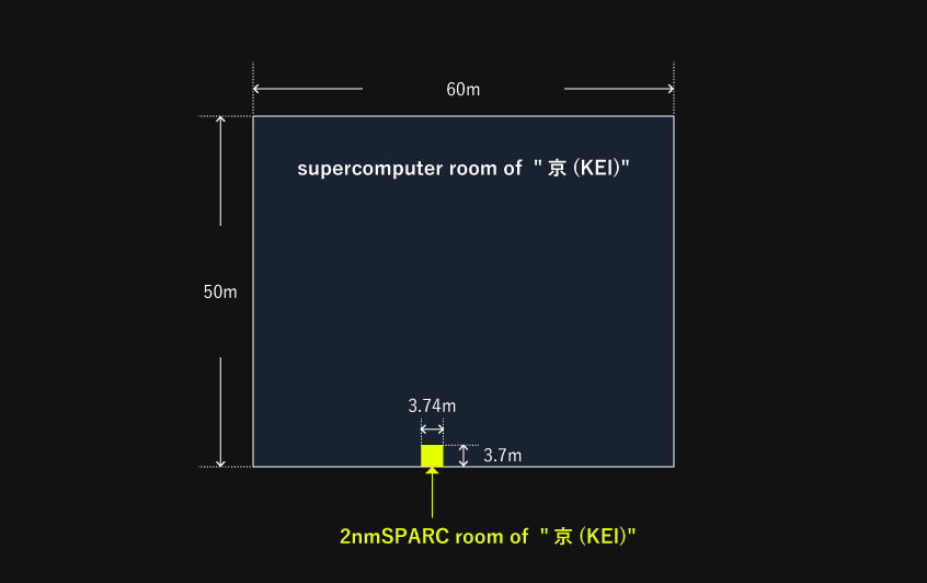
The supercomputer "京(KEI)", which ceased operation in August 2019, had a processing performance of 10.51 PFLOPS(Peta FLOPS). "FLOPS" is an index of a computer's processing power, and indicates the number of floating-point operations that can be performed per second. "Peta" stands for "10 to the power of 15 (1,000 trillion), and 10.51 PFLOPS means that it can process 10,510 trillion operations (≒ 10 quadrillion) per second. 10 quadrillion is called "京(KEI)" in Japan. This is where the name "京(KEI)" comes from. The large 50m x 60m room in which "京(KEI)" is housed is lined with 864 racks. Each rack contains functions such as a calculation unit, communication unit, storage device, cooling unit, and power supply, and the calculation unit uses 102 SPARC64 VIIIfx (hereinafter referred to as SPARC) CPUs. The total number of SPARC processors in the "京(KEI)" computer is 88,128.
Wikipedia. "京(KEI) (supercomputer)".https://ja.wikipedia.org/wiki/京_(スーパーコンピューター),(referred 2024-12-17)
SPARC64 VIIIfx(SPARC)
| Process node | 45nm |
|---|---|
| Chip size | 22.7 mm x 22.6 mm (approx. 513 mm2) |
| Number of transistors | approx.760 million |
| Transistor density | approx.1.5 million transistors per 1mm2 |
| Processing performance | 128 GFLOPS (gigaflops) "G(giga)" stands for "10 to the power of 9 (1 billion)." |
Fujitsu Limited."supercomputer「京(KEI)」CPU SPARC64 VIIIfx". https://www.fujitsu.com/downloads/JP/archive/imgjp/jmag/vol63-3/paper04.pdf, (referred 2024-12-17)
128GFLOPS x 88,128 is about 11.28PFLOPS (= theoretical efficiency), which is almost the same as the processing performance of "京(KEI) computer". Theoretically, the CPU processing power x number of CPUs is overall roughly processing power. The transistor density of the subject 2-nanometer process is said to be about 333.33 million transistors per mm2.
ANANDTECH.「IBM Creates First 2nm Chip」.https://www.anandtech.com/show/16656/ibm-creates-first-2nm-chip,(referred 2024-12-17)
So, how many SPARCs can fit into the 513mm2 area of one 45nm SPARC in a 2-nanometer process?
= 2-nanometer process transistor density x 513mm2 ÷ number of SPARC transistors
= 333.33 million transistors/mm2 x 513mm2 ÷ 760 million transistors
≒ 225
With a 2-nanometer process, 225 SPARCs can fit into 513 mm2. In other words, 225 times the functionality fits into the same area.
= 2-nanometer process transistor density x 513mm2 ÷ number of SPARC transistors
= 333.33 million transistors/mm2 x 513mm2 ÷ 760 million transistors
≒ 225
With a 2-nanometer process, 225 SPARCs can fit into 513 mm2. In other words, 225 times the functionality fits into the same area.
Here, we'll call a chip packed with 225 SPARCs a "2nm SPARC." The processing power of a "2nm SPARC" is approximately 28.8 TFLOPs (teraflops). Tera is 10 to the power of 12 (1 trillion).
Let's compare specific sizes. If the supercomputer "京(KEI)" were built with "2nm SPARC", how much smaller would it be?
The processing performance of "京(KEI)", which uses 88,128 SPARCs, could be achieved with 391 2nm SPARCs. If the rack structure remains the same as "京(KEI)", but 102 "2nm SPARCs" are used per rack, the number of racks can be reduced from 864 to 4. If 27 x 32 racks are arranged in a 50m x 60m room of "京(KEI)", the area of one rack is 1.85m x 1.87m. If 2 x 2 "2nm SPARC" racks are arranged, the room size will be 3.7m x 3.74m.
The same function will be achieved in 1/216th the area. Realizing a huge function of a 50m x 50m in an area of just 4m x 4m - this is the "Amazingness of 2-nanometer semiconductors."
This comparison is limited to area and does not take into account other factors such as CPU architecture, memory layout, power consumption, or heat generation. At present we are not involved in the development of cutting-edge technologies such as 2-nanometer semiconductors, but working on the development of cutting-edge semiconductors such as "2nmSPARC" is one of our goals.
Evolution in semiconductor processes not only means that chips become smaller and more can be produced, but also that chip performance and power efficiency improve. This enables us to provide customers with high-performance, highly functional, power-saving, and space-saving products at the same or lower price.
As a member of the semiconductor industry, we will not miss out on this evolution and will continue to provide this "value" to our customers.
As a member of the semiconductor industry, we will not miss out on this evolution and will continue to provide this "value" to our customers.