ADC
We have a wide range of applications, including audio, industrial, and medical equipment.
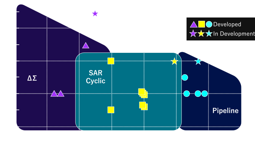
We have a track record of various circuit types for ADCs.
Among them, we have extensive experience with Delta Sigma (ΔΣ), successive approximation (SAR), and pipeline circuit types.
We have a track record of various circuit types for ADCs.
Among them, we have extensive experience with Delta Sigma (ΔΣ), successive approximation (SAR), and pipeline circuit types.
Major ADC development achievements
| Circuit method | Main usage |
|---|---|
| Delta sigma (ΔΣ) | Instrumentation, audio, precision sensors |
| Successive approximation (SAR) | General purpose, microcontroller built-in, low power sensor |
| Pipeline | Industrial/Medical Equipment, Video, Telecommunications |
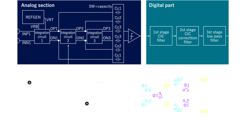
ΔΣADC①
Feature
| Usage | For audio |
|---|---|
| Degree | Tertiary |
| Sampling frequency | 6MS/s |
| Accuracy | 16bit@1KHz input |
| Point | We conduct stable constant and noise designs for the analog component, and optimize the digital component based on the intended use. This configuration applies to audio equipment and similar applications. If the input is DC, it is possible to omit the correction filter, and the low-pass filter can be achieved with only average processing. |
Block Diagram
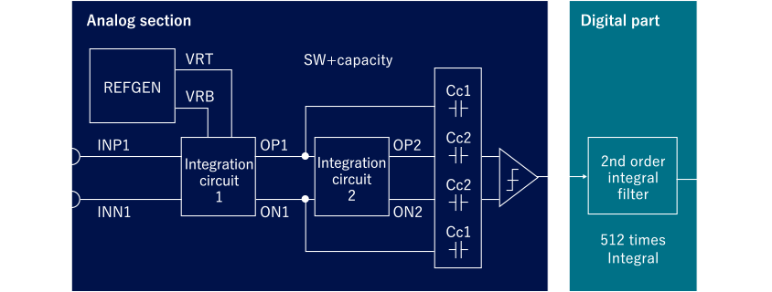
ΔΣADC②
Feature
| Usage | For Temperature sensors |
|---|---|
| Degree | Secondary |
| Sampling frequency | Operates at 8MHz, 512 clocks (for applications where there is no input voltage change during this period) |
| Resolution | 12bit |
| Point | We conduct stable constant and noise designs for the analog component, and optimize the digital component based on the intended use. This configuration applies to audio equipment and similar applications. If the input is DC, it is possible to omit the correction filter, and the low-pass filter can be achieved with only average processing. |
Block Diagram
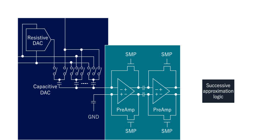
Successive approximation ADC
Feature
| Usage | For MCU |
|---|---|
| Sampling frequency | 1MS/s, 20MHz CLK operation |
| Resolution | 10bit |
| Point |
|
Block Diagram
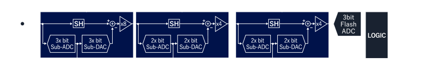
Pipeline ADC
Feature
| Usage | |
|---|---|
| Sampling frequency | 20MS/s |
| Resolution | 12bit |
| Point |
|
Block diagram
Sequential comparison ADC evaluation board system
Functions and features that can be implemented
- The high-speed DAC enables voltage switching at the ADC conversion speed, reducing evaluation time.
- The FPGA can capture vast amounts of ADC data output.
- Any desired waveform can be input to meet specific needs.
- Evaluation equipment and time can be significantly reduced.
- Repetitive measurement is possible.
- After long-term (e.g., 1000 hours) measurement and statistical processing, data can be compressed and output as results.
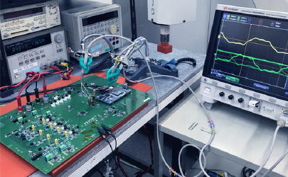
Image
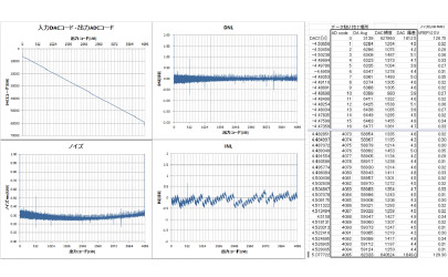
Evaluation result (example)
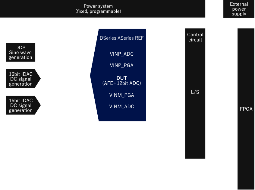
Block Diagram
-
- ADC
- Sensor
- Power management
- Oscillator
- Motor control
- Audio
- Development of a sensor image evaluation system for automotive applications
- Development of a hardware platform for OpenCV implementation in automotive applications.
- Development of industrial camera systems
- CIS digital design
- Digital circuit design for mixed-signal LSI.
- Digital signal processing design