Collaborative Design of Digital and Software (Zynq/Intel SoC)
We are pursuing the technology to optimize the entire system by understanding both digital and software.
Recently, LSI devices equipped with both FPGA and CPU, such as Xilinx's Zynq and Intel's SoC FPGA, are becoming increasingly popular. At SANEI HYTECHS, we conduct digital design for FPGA and software design for CPU, and integrate digital software to operate as one system.Collaborative Design Service for Digital and Software
Issues with Traditional Design
With traditional design, where digital hardware and software are designed separately and then integrated at the end, we have found that we cannot fully utilize the potential of devices like Zynq and Intel SoC. Therefore, it has become necessary to have the technology to understand both digital software and hardware and optimize the entire system as one integrated unit. However, very few engineers possess the necessary expertise.
Benefits of Combining FPGA and CPU onto a Single Chip
The benefits of combining FPGA and CPU, which were previously separated into different chips, onto a single chip are not only that the implementation area becomes smaller and more compact. In Zynq and Intel SoC, communication between FPGA and CPU takes place within the chip, resulting in a significant increase in communication speed. As a result, the bottleneck of communication speed in systems that combine digital software to achieve one function can be removed, which expands the potential for increasing the processing speed of the entire system.
At our company, we are developing a collaborative design service for digital and software. We proactively accumulate technology by creating systems that are likely to have demand on our own, and we can quickly provide necessary design services to customers when specific needs arise.
At our company, we are developing a collaborative design service for digital and software. We proactively accumulate technology by creating systems that are likely to have demand on our own, and we can quickly provide necessary design services to customers when specific needs arise.
Case Studies
Image Recognition System
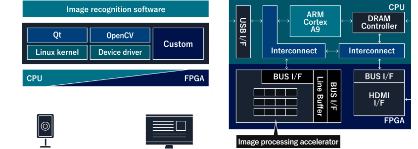
For example, we are developing an "image recognition system" that is currently expanding in the market with a configuration similar to the diagram below.
This system is implemented on a Zedboard (manufactured by AVNET), which is an evaluation board for Zynq.
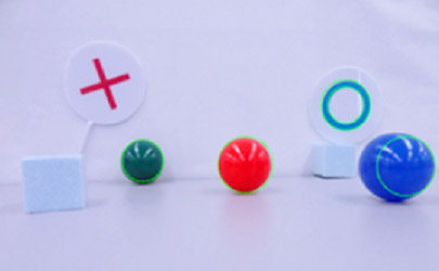
Example image recognition algorithm (circle detection)
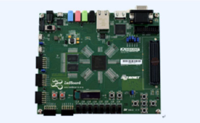
Zynq evaluation board "Zedboard" (manufactured by AVNET)
Optimizing the Entire System to Maximize Performance
The basic part of the image recognition algorithm is processed by software, while part of the processing is extracted and accelerated by digital circuits for faster performance. The software runs on the CPU inside Zynq, while the digital circuit runs on the FPGA inside the same Zynq. Understanding the algorithm and deciding how much to assign to software and which parts to assign to the digital circuit is the key to optimizing the entire system and maximizing performance.
Reducing Development Time by Utilizing Existing Libraries and IPs
In developing such systems, it is important to minimize development time (development period) by utilizing available libraries and IPs as much as possible instead of building everything from scratch. For example, in this system, Linux OS is installed on the CPU, and the software runs on that OS. By using Linux OS, we can use open programming libraries such as Qt (a type of GUI library) and OpenCV (a type of image processing library).
Furthermore, Linux OS provides various device drivers, so even when connecting a USB camera, we can use the USB driver included in Linux OS without having to prepare a dedicated USB interface. On the FPGA side, we obtained high-speed interfaces such as HDMI, which are difficult to realize in software, from Xilinx's website as IPs and integrated them into the system. However, since the image format differs between HDMI and the image recognition algorithm, we created a digital circuit for format conversion and inserted it in front of the HDMI IP.
To efficiently proceed with development, it is also necessary to have the expertise to combine existing IPs and custom circuits effectively.