Digital circuit design for mixed-signal LSI.
Here is an example of digital logic design for mixed-signal LSI, specifically for delta-sigma ADCs.
System overview
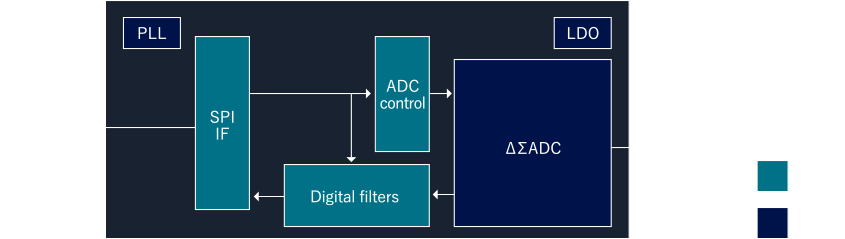
System overview
Here is an example of digital logic design for mixed-signal LSI, specifically for delta-sigma ADCs.
Customer's Request
- Meeting target performance through analog-digital co-design.
- Designing chips with considerations for power reduction and IC testing methodologies.
- Example Digital Functionalities
- Digital Filter, Serial Interface (I2C, SPI), and ADC Control.
- Sequence Control and Non-Volatile Memory Control (eFUSE, OTP).
Proposal Content (Features)
Our design approach involves collaboration with our team of analog circuit designers to create a holistic system design that meets our clients' performance, chip size, and power consumption targets. Development through reuse design is prevalent in the industry. Therefore, we understand the specifications and design assets of the base IC thoroughly, and extract the design and verification differences to address them effectively. This approach is a unique feature of our design process.
- We propose test design solutions such as analog test mode control, SCAN design rule compliance, and built-in eFuse W/R mode.
- Our design approach is flexible, taking into account analog co-design considerations. We separate the RTL and gate design sections to achieve an optimal analog layout.
- We streamline the verification process by constructing a digital-only verification environment that includes an ADC model for testing.
-
- ADC
- Sensor
- Power management
- Oscillator
- Motor control
- Audio
- Development of a sensor image evaluation system for automotive applications
- Development of a hardware platform for OpenCV implementation in automotive applications.
- Development of industrial camera systems
- CIS digital design
- Digital circuit design for mixed-signal LSI.
- Digital signal processing design