LSI Circuit Design/Semiconductor Design
We are responding to the increasingly sophisticated, diverse, and complex demands of LSI/semiconductor design through a comprehensive design system that integrates circuit design and layout design.
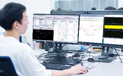
SANEI HYTECHS has a track record as a specialized LSI/semiconductor design company since the dawn of the LSI industry. Today, we provide a comprehensive design system that integrates three businesses: analog circuit design, logic/digital circuit design, and layout design, all working together in collaboration. Our digital and analog circuit designers work together, utilizing tools such as MATLAB/Simulink to design the system as a whole.Furthermore, our layout designers work in close collaboration with analog circuit designers to pursue the reduction of layout area to the limit while realizing circuit characteristics. LSI design requires not only performance but also the ability to meet requirements such as miniaturization and energy efficiency. We strive to achieve the optimal balance between circuit design and layout design, leveraging the latest tools and technologies available.
We understand that the field of LSI design and semiconductor design will continue to advance, diversify, and become increasingly complex in the future. Therefore, we remain at the forefront of technological trends, conducting research and development to swiftly and appropriately respond to our customers' needs.
We believe in the importance of fostering a partnership with our clients, and our mission is to contribute to their success. Our ever-evolving engineering business aims to be a vital force in supporting the advancements of next-generation technologies and becoming an indispensable presence in shaping the future society.
LSI/Semiconductor Design Services
Analog circuit design and verification
Delivering Services to Achieve Performance and Process Limitations and Fulfilling Customer Requirements
We provide services that discern the limits of device performance and process, enabling the realization of required specifications. With a wealth of experience in developing high-performance analog LSIs across various categories such as power management, sensors, ADC, audio, oscillators, and motor control, we have established a solid track record. Our team of analog design experts, nurtured within our company, leverages extensive knowledge and technical assets to meet the high-level requirements of our customers, including semiconductor manufacturers. We prioritize delivering quality and cost-effective solutions that align with our customers' demands.
Logic circuit/digital circuit design and verification
We provide services that enable high performance, miniaturization, and power efficiency through cutting-edge technology.
With our wealth of experience and proven track record, we leverage our expertise to provide services in various stages of FPGA design and logic design, including architecture design, logic verification, and physical verification. We are adaptable to design flows like Waterfall or Agile, tailored to the unique characteristics of each project. To drive efficiency, we utilize the latest languages such as HDL, C/C++, and SystemC, not limited to HDL alone. Furthermore, we are well-equipped to support development methodologies like FPGA development and Model-Based Design (MBD).

LSI Layout Design
We provide services that achieve high-quality and high-value LSIs through skilled layout design.
With our 40 years of experience in manual layout design, we offer a consultative approach to meet the specific needs of our customers. Our strength lies in the seamless integration of analog circuit design and the ability to provide flexible solutions to address challenges.

LSI Evaluation, Analysis
We perform efficient and high-precision evaluation and analysis.
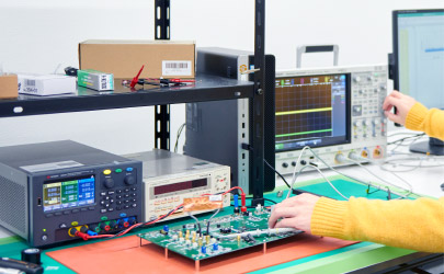
We possess various measurement instruments and not only evaluate LSIs designed in-house but also conduct prototype evaluations of LSIs designed by our clients. Our evaluations of high-performance and multi-functional LSIs are carried out efficiently and with high precision by experienced engineers with extensive circuit design expertise. Through the evaluation process, we provide valuable feedback that contributes to circuit design and layout improvements, ultimately enhancing overall quality.
Analog IC Turnkey Service
Turnkey services for advanced mixed-signal ICs.
We provide turnkey services for mixed-signal ICs, which include both analog ICs and small-scale logic. Depending on our clients' budget and development schedule, we recommend the most suitable fabs from a variety of options, both domestic and international. We are equipped to handle requests for low-volume production and prototyping.

LSI/Semiconductor Design Achievement
LSI/Semiconductor Design Flow
Design phase
-
01
Specification and feasibility study -
02
The LSI design process is as follows. -
03
Layout design
Chip manufacturing phase
-
04
Photomask manufacturing -
05
Wafer manufacturing -
06
Packaging -
07
Prototype evaluation -
08
Test development -
09
Package inspection and reliability testing
Design phase
01Specification and feasibility study
Input
- Required specifications
Process/work
- Specifications study
- Feasibility study
Output
- Design specifications
SANEI HYTECHS has a team of designers who can handle both design and specification considerations. They create design specifications based on the required specifications for LSI development. To achieve the operation and characteristics of the requested system LSI, they design the architecture using tools such as MATLAB/Simulink and functional model verilogA. In mixed-signal LSI development, analog and digital circuits are appropriately integrated and separated during this stage. Our company's distinctive feature is having architecture designers who can efficiently streamline the system LSI design process using a top-down approach.
02Circuit design
Input
- Design specifications
Process/work
- Circuit design
Output
- Design report
- Layout specification
- Prototype evaluation specification
- Test specification
- Circuit data
Based on the design specifications and architecture design, we design circuit parameters. Once the design phase is complete, we use pure SPICE for analog characteristics and AMS for mixed-signal circuits to design and verify them. At SANEI HYTECHS, we use various PDKs from major domestic and international fabs for design verification, and we also develop our own in-house design/verification environment. Furthermore, we actively promote the optimization and streamlining of our design/verification tools.
Analog circuit design and verification
Logic circuit/digital circuit design and verification
Analog circuit design and verification
Logic circuit/digital circuit design and verification
03Layout design
input
- Layout specification
Process/work
- Layout design
Output
- Layout report
- Layout data
- GDS II data
At SANEI HYTECHS, we employ both circuit designers and layout designers who communicate with each other to achieve the smallest possible layout pattern while preserving circuit characteristics. In addition to physical verification, we conduct post-layout simulations as part of the verification process.
LSI Layout Design and verification
LSI Layout Design and verification
Chip manufacturing phase
04Photomask manufacturing
Process/work
- Photomask manufacturing
Output
- Photomask
05Wafer manufacturing
Process/work
- Wafer manufacturing
Output
- Wafer
- Bare chip
06Package processing
Process/work
- Package processing
Output
- Package
07Prototype evaluation
Process/work
- Prototype evaluation
Output
- Prototype evaluation report
At SANEI HYTECHS, we have a team of engineers and access to advanced measurement equipment to conduct comprehensive prototype evaluations of LSIs and semiconductors, whether they are designed by us or by our customers.
08Test development
Process/work
- Test development
Output
- Test program
09Package inspection, reliability test
Process/work
- Package inspection
- Reliability test
Output
- Reliability test report