3nm Semiconductors Explained: Simple Enough for High School Students
2026.02.12
- LSI設計
3-Nano Semiconductors are frequently featured in the news.
Based on our popular "Let's explain to Junior high school students simply! What is a 2-nanometer semiconductor?", we'll explain 3-Nano Semiconductors at a slightly more advanced level for high school students.
Based on our popular "Let's explain to Junior high school students simply! What is a 2-nanometer semiconductor?", we'll explain 3-Nano Semiconductors at a slightly more advanced level for high school students.
Nanometer
3nm (nanometer) is 3 millionths of a millimeter. 3 nanometers is an ultra-fine size—roughly one-thirtieth the size of a virus, which itself is said to be about 1/10,000th of a millimeter.
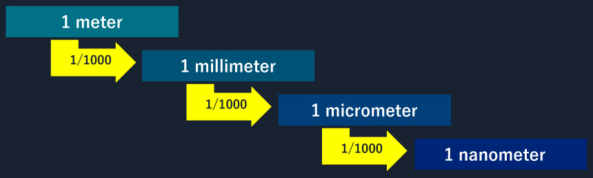
Figure 1 Nanometer
3-Nano Semiconductors
The Meaning of 3 Nanometers
As mentioned in my post "Let's explain to Junior high school students simply! What is a 2-nanometer semiconductor?" the term "3 nanometers" is currently used to mean it is "equivalent to a 3nm process" in terms of performance. Let's explain each one individually.
MOSFET
There are many types of semiconductor transistors, but the most widely used and long-standing transistor is the MOSFET. The MOSFET's greatest feature is its ability to be miniaturized. Over the past 50 years, planar MOSFETs have undergone dramatic miniaturization.
The diagram shows a MOSFET. In Figure 2, the gate is off (no voltage is applied), so no current flows. In Figure 3, the gate is on (voltage is applied), so current flows from drain to source. The presence or absence of gate voltage determines the on/off state of the switch.
The diagram shows a MOSFET. In Figure 2, the gate is off (no voltage is applied), so no current flows. In Figure 3, the gate is on (voltage is applied), so current flows from drain to source. The presence or absence of gate voltage determines the on/off state of the switch.
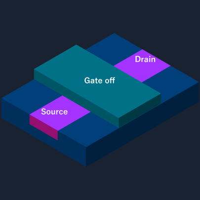
Figure 2 Planar MOSFET (switch off)
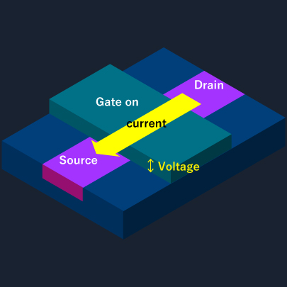
Figure 3 Planar MOSFET (switch on)
Process
The semiconductor manufacturing process is called a "process," and the indicator that represents the miniaturization of semiconductors is called the "process node."
For example, a 45-nanometer process node means that semiconductors are manufactured with a minimum transistor length (L) of 45 nm (nanometers).
The process node is used as an indicator of the performance and integration level of a semiconductor. Over the course of 50 years, planar MOSFETs have dramatically scaled down in process nodes from micro (1/1000 of a millimeter) to nano (1/1,000,000 of a millimeter) following Moore's Law.
*Moore's Law: In 1965, Intel co-founder Gordon Moore proposed Moore's Law, which states that "the density of semiconductor circuits will double approximately every 1.5 to 2 years."
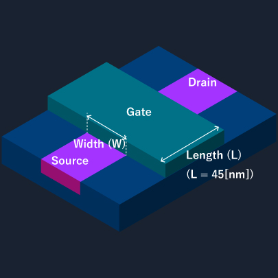
Figure 4 45-nanometer process MOSFET
However, as process nodes approached 22nm, the flat structure of planar MOSFETs could no longer handle this level of miniaturization. This led to issues with leakage current, making it difficult for the transistors to function as proper switches.
This is where the FinFET (Fin-shaped Field-Effect Transistor) comes in. The 3nm FinFET technology is featured in Apple’s M4 chip and is also expected to be produced at a certain leading foundry’s second Kumamoto plant, which is currently under construction.
This is where the FinFET (Fin-shaped Field-Effect Transistor) comes in. The 3nm FinFET technology is featured in Apple’s M4 chip and is also expected to be produced at a certain leading foundry’s second Kumamoto plant, which is currently under construction.
FinFET
By surrounding the thin, fin-shaped element with a gate, FinFETs create a 3D switch. By applying voltage from three sides, it improves performance without needing to shorten the transistor length (L), while also solving the issue of leakage current caused by miniaturization.
Unlike planar types, for FinFETs, the transistor length (L) is no longer a suitable metric for the process node to represent performance or density.
There is not "3 nanometers" in this diagram.
So, what does the "3-nanometer" process node mean? It seems to indicate that the performance and integration density of semiconductors manufactured using this process are equivalent to those of a 3-nm planar MOSFET.
Therefore, the use of "length" in process node names will likely disappear in the future. Intel uses process node names such as Intel7 and Intel3.
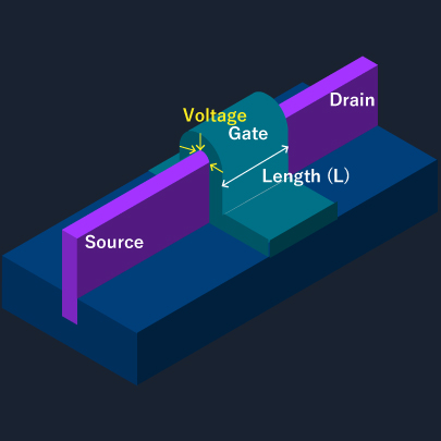
Figure 5 FinFET
Next-Generation Semiconductor Process
Semiconductor processes are constantly evolving. Following FinFET, the "Gate-All-Around (GAA)" MOSFET, used in 2-nanometer semiconductors, has been announced.
Technologies such as RIBBON FET and POWER VIA have been announced for the next angstrom generation.
*Angstrom (Å): 10 billionths of a meter = 0.1 nm
The semiconductor industry has overcome many barriers that were previously thought to be the limits of miniaturization. Furthermore, miniaturization will continue to bring benefits such as high performance, advanced functionality, power savings, and space savings to the world. As a member of the semiconductor industry, we will continue to keep up with process evolution and provide this value to our customers.
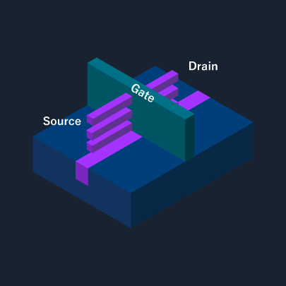
Figure 6 GAA
Reference
- On February 5, 2026, Taiwan's largest semiconductor contract manufacturer, TSMC (Taiwan Semiconductor Manufacturing Company), informed the Japanese government of its plans to become the first in Japan to mass-produce cutting-edge semiconductors with circuit linewidths of 3 nanometers (a nano is one billionth) at its second factory, currently under construction in Kikuyo, Kumamoto Prefecture.
- According to the Yomiuri Shimbun, the Japanese government has decided to provide a subsidy of 732 billion yen for the construction of the second Kumamoto factory. Capital investment is expected to reach $17 billion (approximately 2.6 trillion yen).
- TSMC's 3nm process
- Additional information on semiconductor process rules
https://zenn.dev/takenobu_hs/articles/2acdcd8bce0286