Development of pipeline ADCs/cyclic ADCs
Development of high-performance ADCs.
Our company is engaged in research and development to carry out world-class semiconductor design. We will introduce the process of developing high-performance ADCs (Analog-to-Digital Converters).Development of TEG for ADCs compatible with various sensors
Our company is engaged in the development of ADCs (Analog to Digital Converters) compatible with various sensors. ADCs are necessary circuits that convert physical analog signals received by sensors into digital signals for processing.
Since 2020, we have been developing a 16-bit pipeline ADC/cyclic ADC, and the TEG (Test Element Group) has been completed, with evaluations finished on the evaluation board. We will introduce the process.
The ADC we developed has the performance indicated by the ★ mark in the graph below. The further to the right/upper side of the graph, the higher the performance and the more expensive the ADC becomes.
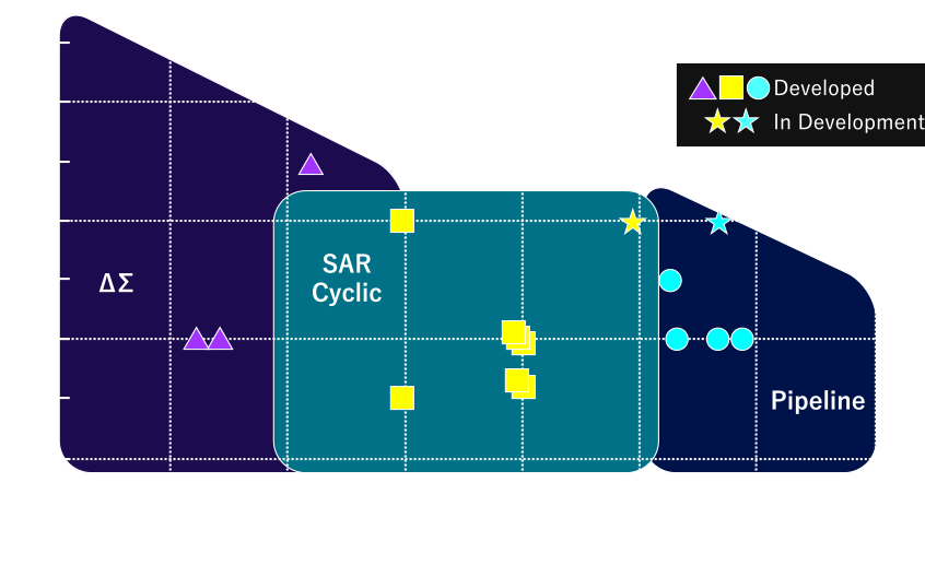
ADC performance areas and San-ei High-Tex's development achievements and plans
The TEG of the developed ADC incorporates the following circuit blocks.
| Pipeline ADC |
|
|---|---|
| Cyclic ADC |
|
| ADC clock system |
|
| High-precision reference voltage |
|
For each circuit block, we are aiming for a significant performance improvement compared to our previous design achievements.
Overview of the prototype TEG (Test Evaluation Board)
The ADC developed by our company has been fully designed in-house, including chip design and layout. In March 2021, the design was taped out for manufacturing.
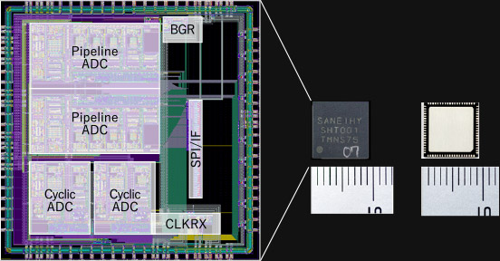
This is an overview of the TEG (test engineering grade) of the prototype ADC.
The major circuit blocks included are:
- TSMC 0.18um (TSMC 0.18-micrometer manufacturing process)
- Total of 4 channels of ADC included
- Package size: 9mm 80-pin QFN package
The major circuit blocks included are:
| 2 channels of pipeline ADC | 16-bit, 50Msps (million samples per second), SNR (signal-to-noise ratio) > 80dB |
|---|---|
| 2 channels of cyclic ADC | 16-bit, 8.5Msps, SNR > 80dB |
| High-precision bandgap voltage reference circuit (BGR) | Temperature trimming, ±0.2% or less |
| SPI/IF and 1024-bit registers for TEG control | Registers for TEG control |
| Clock receiver (CLKRX) | Differential clock receiver for ADC, low jitter + duty correction |
Setting up the evaluation environment
We have developed our own unique evaluation environment which uses FPGA to accelerate data collection/analysis.
The features of the developed evaluation environment are:
The features of the developed evaluation environment are:
- Enables the evaluation of 16-bit, 50Msps ADCs with SNR > 80dB
- Measures both DC characteristics (INL, DNL, etc.) and AC characteristics (SNR, SNDR, SFDR, etc.)
- Allows for high-speed evaluation through FPGA + PC software control
- Each measurement time takes several seconds to one minute
- Requires minimal external evaluation equipment
- Operates with only one DC power supply and a PC
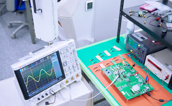
We have created evaluation software using Python.
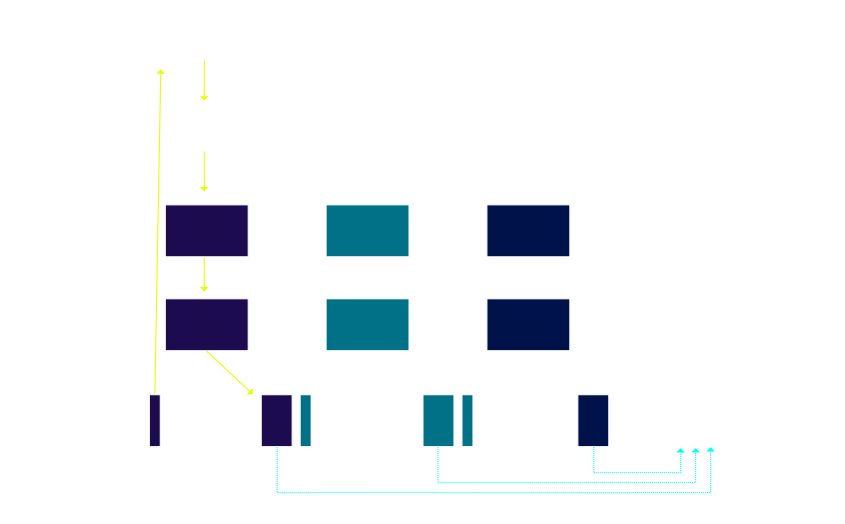
Here is an explanation of the evaluation environment's operation using the example of the Ramp mode during INL/DNL measurement.
When the evaluation software is executed, the following actions occur:
Here is an explanation of the evaluation environment's operation using the example of the Ramp mode during INL/DNL measurement.
When the evaluation software is executed, the following actions occur:
- Python software is launched from the PC's command line
- Communication between the evaluation board and the USB begins, and initial settings are performed
- The following actions are repeated for a specified number of times (3 times in the figure):
- Writes 1 to the FPGA's measurement start register
- The FPGA generates Ramp data and sends the DAC input data
Counts up to 65536 - The DAC outputs a Ramp wave, which passes through the Amp and enters the TEG's ADC
- The ADC output code is received by the FPGA
- The FPGA sequentially stores the results in the DRAM on the evaluation board
- When data for 65536 counts is collected, the measurement is completed and the data is read collectively through USB to the PC
- The measurement data is aggregated and statistical processing such as averaging is performed
- The results are output to a CSV file
- The INL/DNL are calculated by loading the CSV file into Excel
Evaluation results
We conducted TEG evaluation from November 2021.
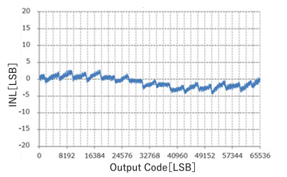
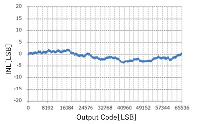
DC Characteristics (INL/DNL) Measurement Results
Here are the measurement results for DC characteristics (INL/DNL).
- Measured using Ramp wave input mode with DAC
- 65536 points were swept, averaged 100 times
Pipeline ADC CH2
DNL - Output Code
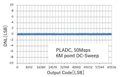
INL - Output Code
Cyclic ADC CH4
DNL - Output Code
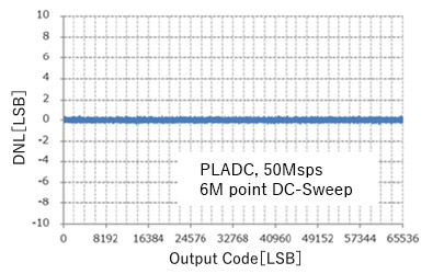
INL - Output Code
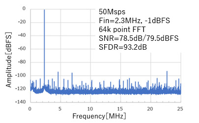
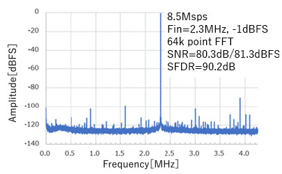
AC Characteristics (SNR/SFDR) Measurement Results
Here are the measurement results for AC Characteristics (SNR/SFDR).
- Measured using sine wave input mode with DDS
- 65536 points were FFT analyzed, averaged 20 times
Pipeline ADC CH2
FFT(PLADC)
Cyclic ADC CH4
FFT(CYADC)
Overall, the evaluation results were generally in line with the target specifications. We will analyze the difference between the design values and the evaluation values and reflect them in the next design.
We have conducted the development and evaluation of high-performance pipeline and cyclic ADCs, which includes not only the design of semiconductor circuits but also the actual IC prototyping, development of evaluation environments, and evaluation.
In the field of analog circuits, which is our specialty, it is difficult to achieve device performance as per the design values due to the influence of factors such as device mismatch, noise from power supply and substrate, and parasitic resistance and capacitance. We pursue technologies that minimize the influence of external factors and confirm the results through evaluation, which is essential for research and development of world-class technologies. We will continue to anticipate the rapidly changing future of the semiconductor industry and meet your expectations.
We are currently looking for engineers to join us in the development process.