Development of Peripheral Circuits for ADC IP (PGA, BGR, RCOSC)
Peripheral IP Development for Maximizing ADC IP Performance | PGA, BGR, and RCOSC
SANEI HYTECHS is developing peripheral circuits compatible with Analog-to-Digital Converter (ADC) IP. This allows us to provide optimal solutions to customers who demand higher precision and performance. Peripheral circuits such as clocks, reference voltages, and buffers for driving input capacitance are essential to operate ADC IP. Below, we will introduce an overview and features of these peripheral circuits.
The Importance of ADC IP Peripheral Circuits
Peripheral circuits that supply the necessary signals are indispensable for ADC IP. To maximize the performance of our high-performance ADC IP, we are concurrently developing crucial peripheral circuit IP, including PGA (Programmable Gain Amplifier), BGR (Bandgap Reference), and RCOSC (RC OSCillator). These peripheral IP enable seamless connection to various sensors, facilitating high-precision and high-efficiency signal processing.
We offer three main peripheral IP:
We offer three main peripheral IP:
- PGA(Programable Gain Amplifier)
- BGR(BandGap Reference)
- RCOSC(Resister-Capacitor OSCillator)
Performance and Features of Peripheral IP for ADC IP
Our peripheral IP have been prototyped and evaluated to confirm their performance. Please refer to the sections for each element for detailed features.
| Element name | Contents and performance (design value) | Features |
|---|---|---|
| PGA | Instrumentation AMP and ADC Input buffer x1 to x128 |
|
| BGR | High Accuracy Bandgap 1.0V 0.2% 3.3V |
|
| RCOSC | High Accuracy RCOSC 5-80MHz 1.5% 1.8V |
|
Other in-house developed ADC IP characteristics
We have developed highly original ADC technology and provide it to our customers, taking advantage of our many years of research and development and extensive experience. Detailed characteristics of other in-house developed ADC IP can be viewed at the link below.
PGA Features
Typically, PGA (Programmable Gain Amplifier) require dedicated customization to perfectly match the circuits they're connected to at both the input and output. At SANEI HYTECHS, we can design custom circuits tailored to your specific needs, leveraging your existing IP, our proprietary IP, and advanced technologies.
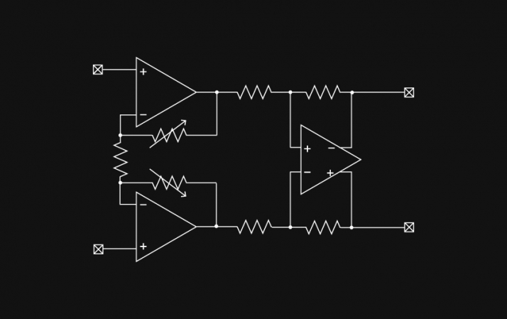
Here, we'll introduce a PGA IP specifically designed for our in-house developed SARADC and OS-SARADC IP. This PGA IP functions as an input buffer for the ADC and boasts the following key features:
Here, we'll introduce a PGA IP specifically designed for our in-house developed SARADC and OS-SARADC IP. This PGA IP functions as an input buffer for the ADC and boasts the following key features:
High-Speed Driving Capability
Drives the ADC's input capacitance at speeds up to 10MHz, enabling high-speed signal processing.High-Impedance Input
Its high impedance allows sensors that cannot be directly connected to a SARADC to be connected via the PGA.Circuit Configuration
Composed of an instrument amplifier and a fully differential buffer circuit, achieving a wide input common-mode voltage range and stable amplification gain.Variable Gain
The gain can be varied from 1x to 128x, allowing small sensor signals to be reliably amplified and passed to the ADC.Auto-Zero and Chopping Function
Equipped with auto-zero and chopping functions, it achieves signal processing that minimizes offset and 1/f noise generated in the PGA.Optimized Power and Noise Performance
The power consumption and noise level of this PGA are optimized to match the SARADC's performance, resulting in highly efficient operation.PGA block diagram
BGR Features and Evaluation Results
The BGR (Bandgap Reference) is a circuit designed to output a reference voltage with minimal fluctuations due to temperature or power supply voltage changes. SANEI HYTECHS' BGR IP is particularly optimized for low temperature dependency, making it ideal as a reference voltage for temperature-sensitive sensors.
Below are its main features:
Below are its main features:
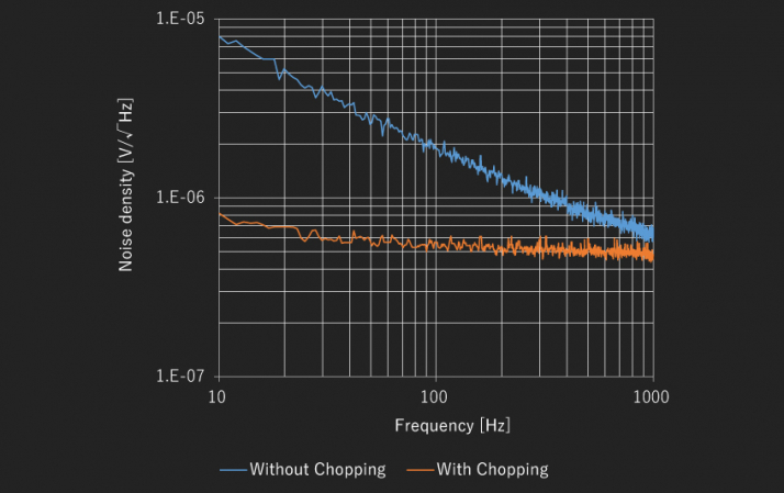
Chopping function
The chopping function can be enabled or disabled. When activated, the chopping function effectively suppresses individual output voltage variations and significantly reduces 1/f noise. Should chopping not be required, it can be deactivated.Output Voltage Single-Point Trimming
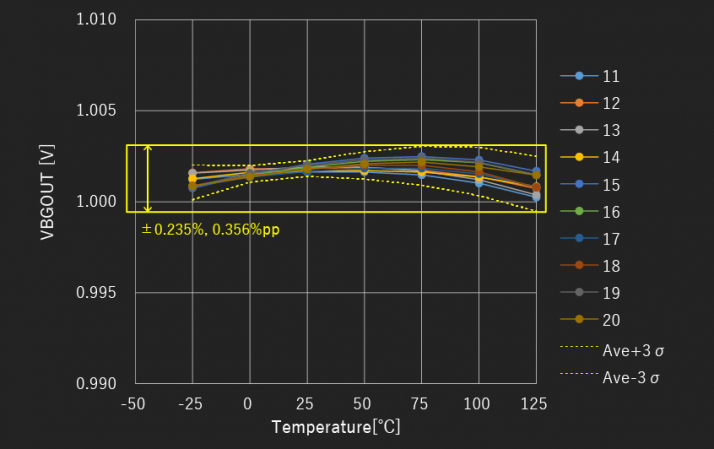
Typically, trimming involves measuring voltage at two temperature points to determine the trimming code. This BGR circuit is designed so that the trimming code can be determined by measuring the voltage at a single point at 25°C, making it easy to adjust at the time of shipment.BGR Evaluation Results
SANEI HYTECHS has conducted performance evaluations of our BGR using prototyped IC. Representative evaluation results are shown below:
Please feel free to contact us for evaluation results under different conditions.
Please feel free to contact us for evaluation results under different conditions.
Conditions: 3.3V, 10 samples, trimmed at one point for 25℃ output voltage.
Output noise density
RCOSC Features and Evaluation Results
The RCOSC (Resistor-Capacitor OSCillator) is an oscillation circuit that generates a clock using resistive and capacitive elements. SANEI HYTECHS' RCOSC IP is ideal as a reference clock for sensors sensitive to clock frequency changes, as its fluctuations due to power supply voltage and temperature are extremely small.
Here are its main features:
Here are its main features:
Reduced Power Supply Voltage and Temperature Dependence
The circuit design incorporates innovations to minimize factors that cause variations with changes in power supply voltage and temperature. This enables the output of a stable clock that is highly resilient to power supply voltage and temperature fluctuations.Long-Term Output Frequency Stability
The design minimizes the effects of offset and aging in internal comparators and operational amplifiers, ensuring a stable clock frequency over extended periods.Ingenious Trimming Function
By simply trimming at one point within the setting frequency, also the other settings will be switched and adjusted. Trimming at just one point of the set frequency automatically adjusts and optimizes all other settings. For instance, if you trim to 40MHz, switching the setting to 80MHz will result in virtually no frequency deviation. This makes frequency trimming incredibly straightforward.Reduced Current Consumption at Low Frequencies
By setting a lower oscillation frequency, it is possible to simultaneously reduce current consumption.Spread Spectrum Function
Enabling the spread spectrum function reduces the peak of the output signal's frequency components, thereby contributing to electromagnetic interference (EMI) countermeasures.Evaluation results of RCOSC
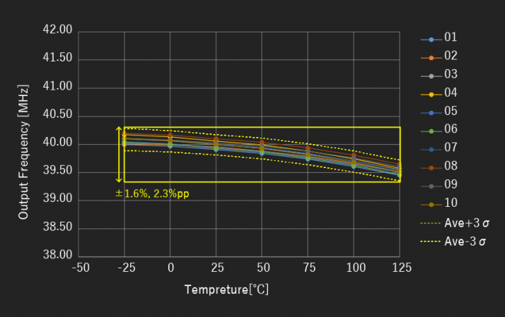
We have evaluated the performance of our RCOSC using prototyped IC. Here are the representative evaluation results:
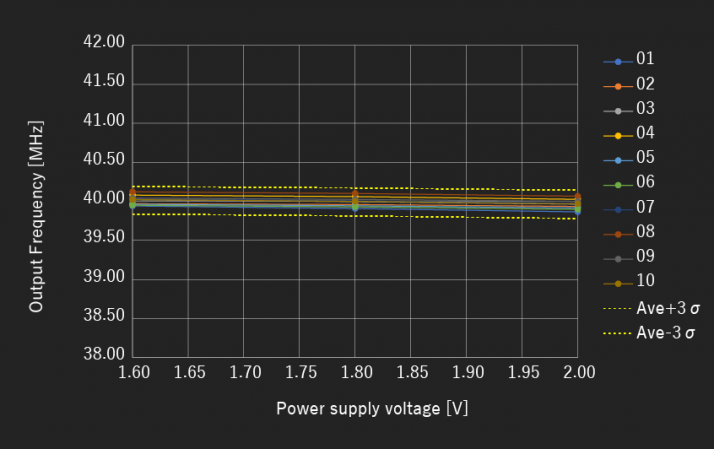
Evaluation Result: We verified that the accuracy remains consistent even after trimming at 40MHz and then reconfiguring to 80MHz.
We also have evaluation data for different conditions. If you are interested in detailed evaluation results or performance under specific conditions, please feel free to contact us.
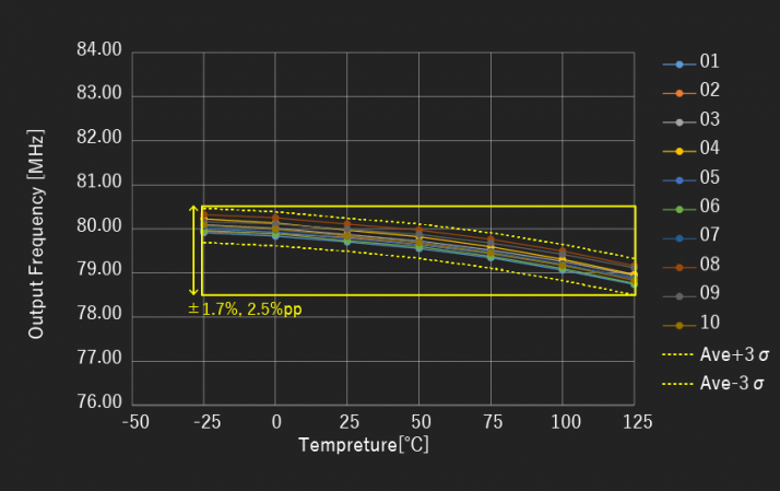
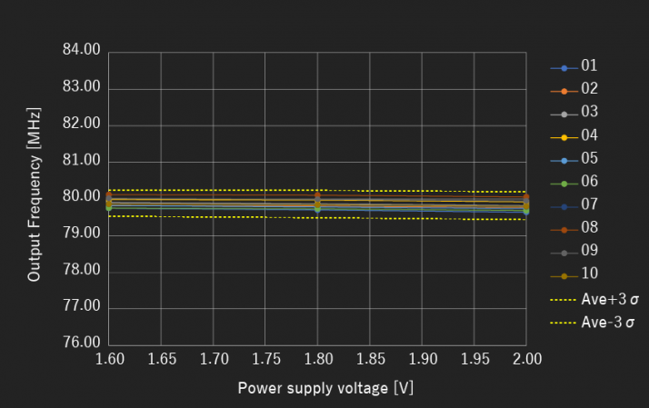
40MHz Output @ 40MHz Trimming
Temperature Drift Characteristics at 1.8V (10 Samples)
Power Supply Voltage Variation Characteristics at 25℃
80MHz output @40MHz trimming
Temperature Drift Characteristics at 1.8V (10 Samples)
Power Supply Voltage Variation Characteristics at 25°C
IP provision and process porting
We also provide own IP at ADC IP peripheral circuits. We can also port to your required process. We can customize to meet your needs, so please consider using it together with ADC IP and custom circuit design. We may also be able to provide IP for not listed. If you need a IP, please feel free to contact us.